For years, the PC industry has encouraged users to mix and match CPUs, expansion cards, RAM, and other components in order to build a modular, extensible platform. Now, under what’s known as Universal Chiplet Interconnect Express, or UCIe, a collection of firms aims to accomplish it at the chip level.
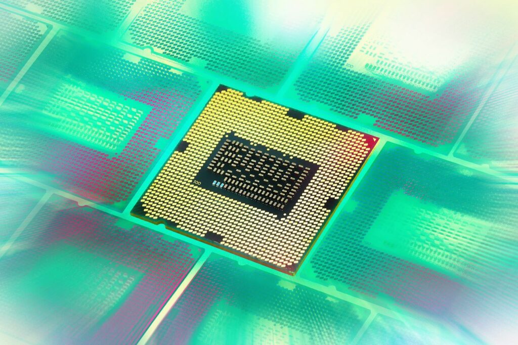
UCIe extends the notion of “chiplets”—individual bits of self-contained logic sewn together inside a chip package—to the whole semiconductor industry. AMD and Intel have been doing this for years, with Intel’s co-EMIB and ODI connections providing the world with its hybrid processor, Alder Lake. The “Kaby Lake G” Intel CPU includes an AMD GPU thanks to a particular engineering relationship between AMD and Intel.
UCIe specifies the Physical Layer (Die-to-Die I/O) and protocols for chiplet interfaces, which now include PCIe and CXL (Compute Express Link), although more protocols will be introduced in the future.
The purpose is to make it possible to mix and match package dies from different fabs, designs/architectures, and packaging methods. The goal of the endeavour, according to the Universal Chiplet Interconnect Express, is to meet the rising needs for compute, memory, and storage in the cloud, edge, corporate, 5G, automotive, increased processing, and hand-held sectors.
UCIe is a chip meant to make the production of a future “Kaby Lake G” chip much easier. The current PCI Express standard or the associated CXL (Compute Express Link) interface used by data centres are both utilised by UCIe to transport data. In essence, a chip maker might take a CPU core from one firm, a graphics core from another, and a WiFi radio or 5G radio front-end from a third semiconductor company, and snap them together like LEGO pieces using UCIe, similar to how a graphics card or SSD can be inserted into a PC’s PCI Express slot. This would be done at the chip level using UCIe. [There’s more in a UCIe white paper (PDF).]
AMD, Arm, Advanced Semiconductor Engineering, Inc. (ASE), Google Cloud, Intel, Meta/Facebook, Microsoft, Qualcomm, Samsung, and TSMC are among the UCIe supporters. Nvidia is the one exception, since it has yet to publicly sign on.
The new standard is also a surrender of sorts, acknowledging that today’s design demands are just beyond the industry’s capacity to physically build them. For decades, the PC industry has attempted to build all-in-one PC processors with a CPU, GPU, I/O, and other features all on a single chip. However, as chips get bigger and bigger, there’s a greater chance of lithography defects, which might render the chip useless. Indeed, UCIe is designed to prepare for the day when new hybrid chips become too huge to create with today’s lithographic equipment.
UCIe, in theory, would let anybody with the necessary permissions and intellectual property to put together a chip package combining logic from a variety of firms. UCIe also indicates that a variety of small businesses may create specialised logic, package it with a UCIe interface, and sell it to other semiconductor firms.